
 Chinese (Simplified)
  English (UK)
  French
  German
  Spanish
  Swedish
 Selective Plating for the Semiconductor Industry
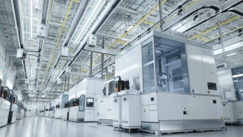
Areas on CVD tooling and steel enclosures used in Semiconductor manufacturing can be enhanced or repaired using the SIFCO Process to selectively electroplate localized areas, quickly and uniformly, before the components go into production, or once they get worn out.
To prevent wear and provide corrosion protection on aluminum, CVD tooling manufacturers usually need a thin layer of nickel. Steel enclosure manufacturers design the framework for the CVD processing equipment, which also require a selective layer of zinc to specific exposed areas to create grounding areas used in the electrical panel cabinet.
By using the SIFCO Process® for selective plating, it ensures semiconductor manufacturers can comply with specifications from companies including Applied Materials and LAM Research. When compared to other electroplating processes, selective plating can apply these deposits locally, which helps manufactures minimize production downtime and increase the lifecycle of not only each component but the front-end vapor deposition equipment and complete semiconductor machine.
Selective Plating and Semiconductor Chamber Components
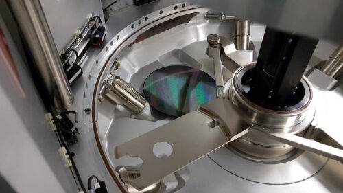
Nearly all semiconductor manufacturing equipment utilizes chemical vapor deposition (CVD). CVD is a technology used for forming solid powders in the gas phase or depositing films on substrates from precursors in the gas phase. CVD uses source materials that flow into the process chamber from external reservoirs that can be refilled without contamination of the growth environment, and it does not require high vacuum levels.
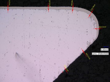
These chambers are typically made from 6061 aluminum alloy and are hard coat anodized. Once anodized, certain areas are machined to ensure a proper seal. For example, the o-ring groove of one such chamber was 3.15 mm wide and 2.63 mm deep after machining.
The groove then required a thin layer of Nickel 2080 and 2807 for corrosion protection of the exposed area. With the SIFCO Process® of selective plating the groove was able to be masked off and selectively plated without damaging any adjacent areas – significantly minimizing production downtime.
 Benefits of Using the SIFCO Process® on Semiconductor Manufacturing Equipment:
There are many challenges facing the semiconductor sector, including manufacturing enough to try to meet demand. This means that minimizing any production downtime, and also maximizing the lifetime of the components. This is where selective plating using the SIFCO Process® can help, other benefits include:
- Portable process
- Minimal masking and disassembly
- 60x faster than tank plating
- Increase service life
- Superior technical expertise
- Quality plating results